
PCB Manufacturing Process: From Gerber Files to Final Delivery
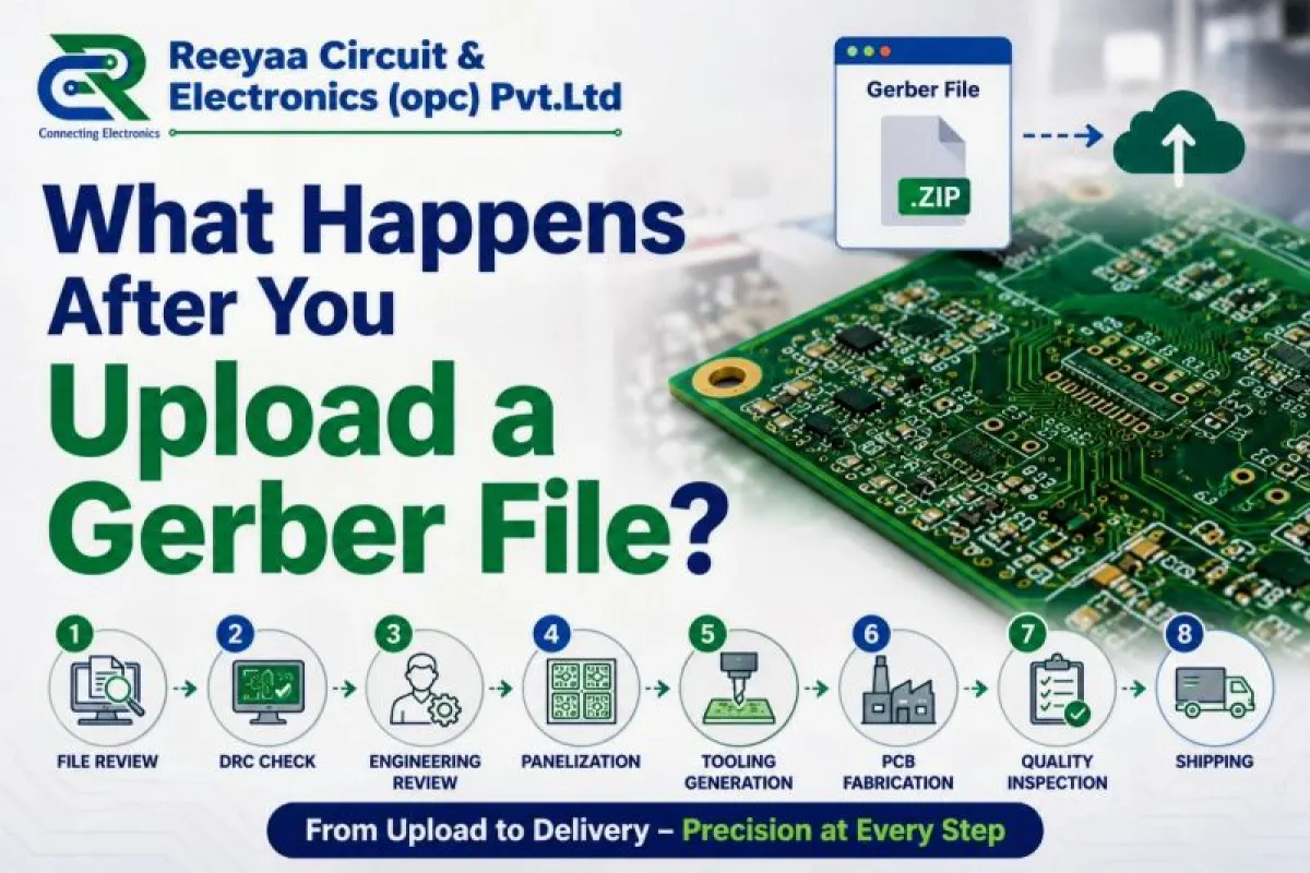
Most engineers think their job is done once the Gerber file is uploaded.
In reality, that's where the manufacturing journey begins.
Every week, we receive dozens of PCB designs from startups, R&D teams, students, and product companies. While the final board may look simple, a lot happens between "Upload Gerber" and "PCB Delivered."
Here's a quick look behind the scenes:
🔍 File Review & DRC
The first thing we do is check whether the design can actually be manufactured. Trace widths, clearances, drill sizes, solder mask openings—everything gets verified before production starts.
🛠️ Engineering Review
Our CAM team reviews the files and prepares them for manufacturing. Sometimes minor issues are identified before they become expensive problems on the production floor.
💡 Interesting Fact: PCB dimensions are often compensated slightly during manufacturing because FR4 material can expand or shrink during processing.
📐 Panelization & Tooling
Your PCB is arranged on a larger production panel. Machine programs are then generated for drilling, routing, imaging, and testing.
🏭 Fabrication
This is where the board comes to life through multiple processes including imaging, etching, copper plating, solder mask application, and silkscreen printing.
✅ Inspection & Electrical Testing
Before shipping, every board goes through quality checks. Flying Probe Testing helps identify opens, shorts, and connectivity issues that may not be visible to the eye.
📦 Shipping
Only after passing inspection does the PCB get packed and dispatched.
One of the most common reasons for production delays?
Missing or incomplete manufacturing files.
Recently, a customer requested an urgent prototype build, but the board outline layer was missing from the Gerber package. It was a quick fix, but it still delayed production while we waited for clarification.
A clean Gerber package doesn't just help your manufacturer—it helps you get your boards faster.
Have you ever encountered a Gerber file issue that caused an unexpected delay? I'd love to hear your experience.
Related Articles

Choosing the Right PCB Copper Weight: 1 oz vs 2 oz vs 3 oz
Learn the differences between 1 oz, 2 oz, and 3 oz PCB copper weights, including copper thickness, current-carrying capacity, trace width, and applications. Discover how to select the right copper weight for digital circuits, power supplies, motor controllers, and EV electronics.
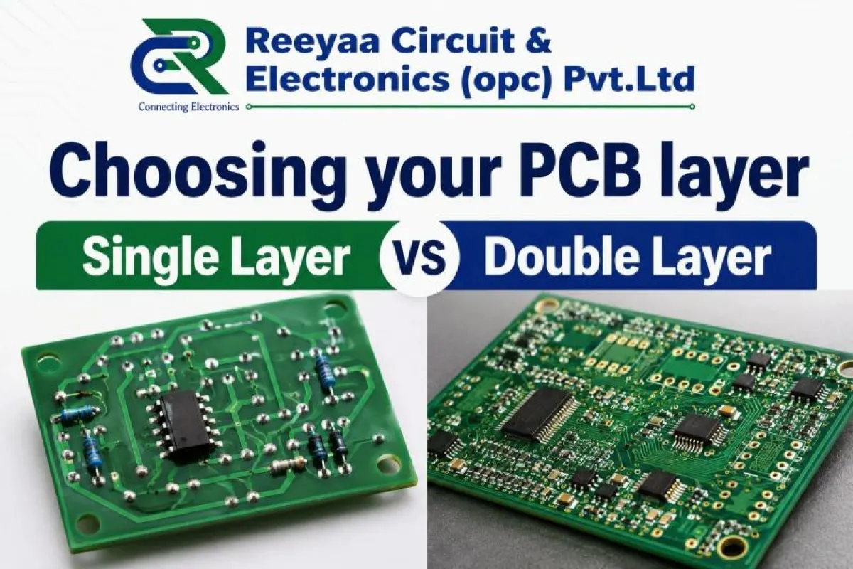
Single Layer vs Double Layer PCB: Which One Should You Choose?
Understand the differences between single-layer and double-layer PCBs, including cost, design complexity, space efficiency, and applications. Discover which PCB type best suits your electronic project.
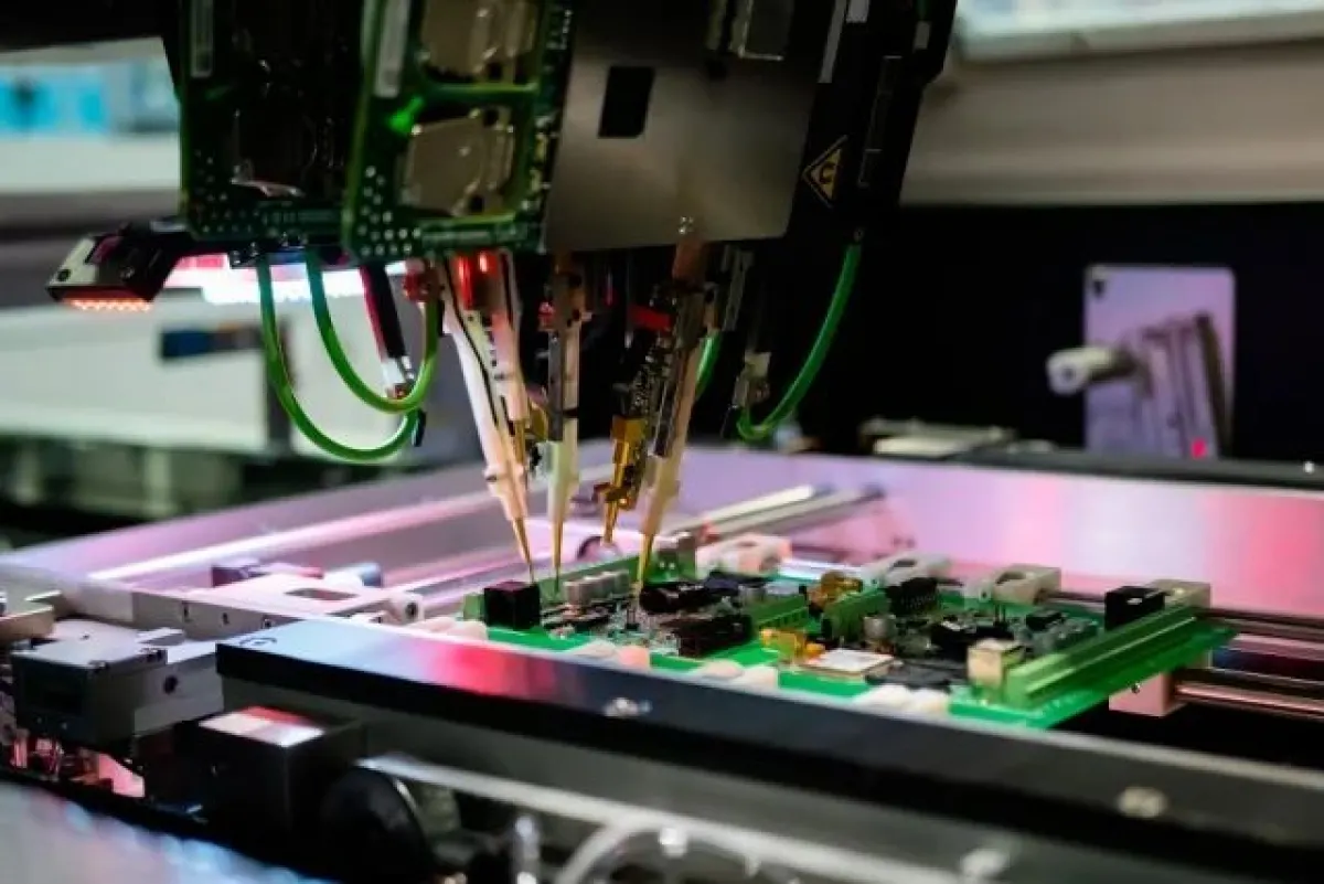
Flying Probe Testing (FPT): Ensuring PCB Quality at Reeyaa Circuit
Discover how Reeyaa Circuit uses Flying Probe Testing (FPT) to detect electrical opens and shorts in bare PCBs. Reliable electrical testing helps ensure PCB quality before component assembly.