
Why a DFM Review is Your Best Insurance Against PCB

There is a unique kind of frustration that every hardware engineer knows too well: you spend weeks perfecting a schematic, routing traces late into night, running your final DRC (Design Rule Check) in your CAD software, and proudly export your Gerber files. You upload them to your manufacturer, feeling ready to test your hardware next week.
Then, the email arrives: “Production on hold. Clearance violation on layer 2.”
Suddenly, your timeline slips by days or even weeks. You have to patch the layout, re-export, and wait all over again.
This exact scenario is why a rigorous Design for Manufacturing (DFM) review is not just an optional formality—it is the single most important step to protect your project budget and schedule.
What Actually Happens During a DFM Review?
Many designers assume that if a CAD tool’s internal DRC passes without errors, the board is automatically ready for the factory floor. Unfortunately, software design rules do not always account for the laws of physics and chemical processing.
When your files land at a fabrication facility like Reeyaa Circuit, an experienced CAM (Computer-Aided Manufacturing) engineer and automated systems inspect your package for real-world manufacturing constraints:
-
Acid Traps and Acute Angles: Sharp 90-degree or acute trace corners can trap etching chemicals during the chemical milling stage, leading to over-etching, thinning tracks, or accidental open circuits.
-
Annular Ring Integrity: If a drill hole is slightly misaligned during mechanical CNC drilling, an insufficient annular ring around the via pad can break the electrical connection. DFM ensures adequate copper pad size around every hole.
-
Trace-to-Copper and Solder Mask Clearances: Chemical etching and mask application have physical tolerances. Tracks running too close to copper pours or pads can bridge during soldering if clearances are too tight.
-
Board Outline and Routing Conflicts: Missing drill files, unclosed board outlines, or overlapping mechanical layers can stall automated CNC routing before milling even begins.
The Hidden Costs of Skipping DFM
When these microscopic errors go unnoticed until manufacturing begins, the consequences compound quickly:
-
Scrap and Material Waste: Once etching or drilling starts on incorrect parameters, the raw FR4 laminate cannot be salvaged. The panel becomes scrap, requiring an entirely new production run.
-
Stalled Firmware and Testing: Your physical hardware holds up firmware development, mechanical enclosure testing, and lab validation. A one-week board delay can push your entire product release cycle back by a month.
-
Unexpected Financial Overhead: Re-spinning a board means paying for tooling, setup, and expedited shipping a second time.
Practical DFM Habits for Hardware Designers
You can minimize production back-and-forth by keeping a few practical rules in mind before exporting your files:
-
Respect Standard Capabilities: Stick to standard limits unless your design strictly demands high-density interconnects (HDI). Standard manufacturing limits—such as 4 mil (0.1 mm) trace widths and 10 mil (0.25 mm) finish hole sizes—drastically reduce production risks for single-sided and double-sided boards.
-
Verify Your Silkscreen: Ensure component designators do not overlap with bare copper pads or through-holes. Solder mask will clip text that crosses pads, making assembly confusing.
-
Double-Check Your Drill and Outline Layers: Always ensure your NC drill file uses the same coordinate units (inches or millimeters, leading/trailing zero suppression) as your Gerber export.
How We Handle DFM at Reeyaa Circuit
We believe that transparency and speed should go hand-in-hand. When you upload your Gerber files directly to our online ordering portal at app.reeyaacircuit.com, our system automatically detects your board dimensions and project parameters, allowing you to select your specifications and quantities in minutes.
Operating out of our ISO 9001:2015 certified manufacturing facility in Gandhinagar, Gujarat, our engineering team reviews your design files to catch potential manufacturing roadblocks early. Combined with our 100% Flying Probe Testing (FPT) on every single board—whether you order a single urgent prototype or a bulk production batch—we make sure your hardware arrives working, on time, and within budget.
Don't let avoidable design rule errors derail your next engineering milestone. Design smart, verify your files, and partner with a manufacturer who has your back.
Frequently Asked Questions (FAQs)
Q1: Is a CAD Design Rule Check (DRC) the same as a DFM review?
A: Not quite. A CAD DRC checks your layout against the rules you set in your software. A DFM review checks your files against the actual physical, chemical, and mechanical limitations of the manufacturing equipment on the factory floor.
Q2: What is the most common DFM error that delays PCB production?
A: Missing board outline layers, unclosed contour lines, and drill-to-copper clearance violations are among the most frequent issues caught during initial file reviews.
Q3: Can DFM checks be automated?
A: Automated software catches many dimensional and clearance errors instantly, but complex geometries, acid traps, and thermal relief issues still benefit greatly from experienced CAM engineering oversight.
Q4: How does Reeyaa Circuit handle DFM issues found in my files?
A: If our engineering team identifies a critical design discrepancy that could cause a manufacturing defect, we flag it and communicate with you promptly to get your approval before production begins.
Internal Link Recommendations
Related Articles

Choosing the Right PCB Copper Weight: 1 oz vs 2 oz vs 3 oz
Learn the differences between 1 oz, 2 oz, and 3 oz PCB copper weights, including copper thickness, current-carrying capacity, trace width, and applications. Discover how to select the right copper weight for digital circuits, power supplies, motor controllers, and EV electronics.

PCB Manufacturing Process: From Gerber Files to Final Delivery
Discover how a PCB moves from Gerber file submission to final delivery. Learn about design rule checks, CAM engineering review, panelization, fabrication, electrical testing, and common causes of production delays.
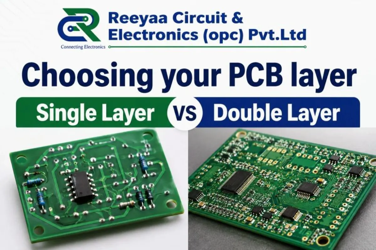
Single Layer vs Double Layer PCB: Which One Should You Choose?
Understand the differences between single-layer and double-layer PCBs, including cost, design complexity, space efficiency, and applications. Discover which PCB type best suits your electronic project.