
Choosing the Right PCB Copper Weight: 1 oz vs 2 oz vs 3 oz

Choosing the Right 𝗖𝗼𝗽𝗽𝗲𝗿 𝗪𝗲𝗶𝗴𝗵𝘁 (𝟭 𝗼𝘇 𝘃𝘀 𝟮 𝗼𝘇 𝘃𝘀 𝟯 𝗼𝘇)
Ever wonder why 𝗣𝗖𝗕 𝗰𝗼𝗽𝗽𝗲𝗿 𝗶𝘀 𝗺𝗲𝗮𝘀𝘂𝗿𝗲𝗱 𝗶𝗻 𝗼𝘂𝗻𝗰𝗲𝘀 instead of millimeters?
As a manufacturing company, We see a lot of boards come through our facility. Picking the wrong copper weight is a quick way to either overspend on materials or literally fry your board under load.
Here is what it means and how to choose the right one for your next project:
What is Copper Weight?
In PCB fabrication, "1 oz copper" means exactly 1 ounce of solid copper rolled out flat over 1 square foot. This translates into a precise physical thickness:
𝟭 𝗼𝘇: 𝟭.𝟯𝟳 𝗺𝗶𝗹𝘀 𝗼𝗿 𝟯𝟱 μ𝗺
𝟮 𝗼𝘇: 𝟮.𝟳𝟰 𝗺𝗶𝗹𝘀 𝗼𝗿 𝟳𝟬 μ𝗺
𝟯 𝗼𝘇: 𝟰.𝟭𝟭 𝗺𝗶𝗹𝘀 𝗼𝗿 𝟭𝟬𝟱 μ𝗺
𝗛𝗼𝘄 𝘁𝗼 𝗖𝗵𝗼𝗼𝘀𝗲 𝗬𝗼𝘂𝗿 𝗪𝗲𝗶𝗴𝗵𝘁
The thickness of your copper directly determines how much current a trace can carry without overheating.
𝟭 𝗼𝘇 (𝟯𝟱 μ𝗺): The Industry Standard. Best for everyday digital routing, microcontrollers, and IoT devices. It allows us to safely etch very fine traces, including a minimum track width of 4 mil (0.1 mm). If your board is mostly processing signals, stick with 1 oz.
𝟮 𝗼𝘇 (𝟳𝟬 μ𝗺): The Heavy Lifter. Moving power? You need 2 oz. It is ideal for motor controllers, power supplies, and EV electronics where higher currents run through the board. Thicker copper handles amperage effortlessly and dissipates heat much better.
𝟯 𝗼𝘇+: Extreme Power. Reserved for heavy industrial applications, high-power converters, and heavy EV chargers. Keep in mind: the thicker the copper, the wider your spacing between traces needs to be to prevent shorting during the chemical etching process.
How 𝗥𝗲𝗲𝘆𝗮𝗮 𝗖𝗶𝗿𝗰𝘂𝗶𝘁 Can Help
Operating out of our manufacturing facility in Gandhinagar, Gujarat, we regularly fabricate Single Side and Double Side PCBs with both 1 oz (35 µm) and 2 oz (70 µm) finish copper thicknesses.
The moment your Gerber files arrive, we run Design Rule Checks (DRC) to catch physical impossibilities, ensuring your trace widths and clearances make sense. Plus, every board undergoes 100% Flying Probe Testing (FPT) to guarantee those power lines are flawlessly connected.
What is the heaviest copper weight you have ever had to route on a tight design? Share in the comments!
Related Articles

PCB Manufacturing Process: From Gerber Files to Final Delivery
Discover how a PCB moves from Gerber file submission to final delivery. Learn about design rule checks, CAM engineering review, panelization, fabrication, electrical testing, and common causes of production delays.
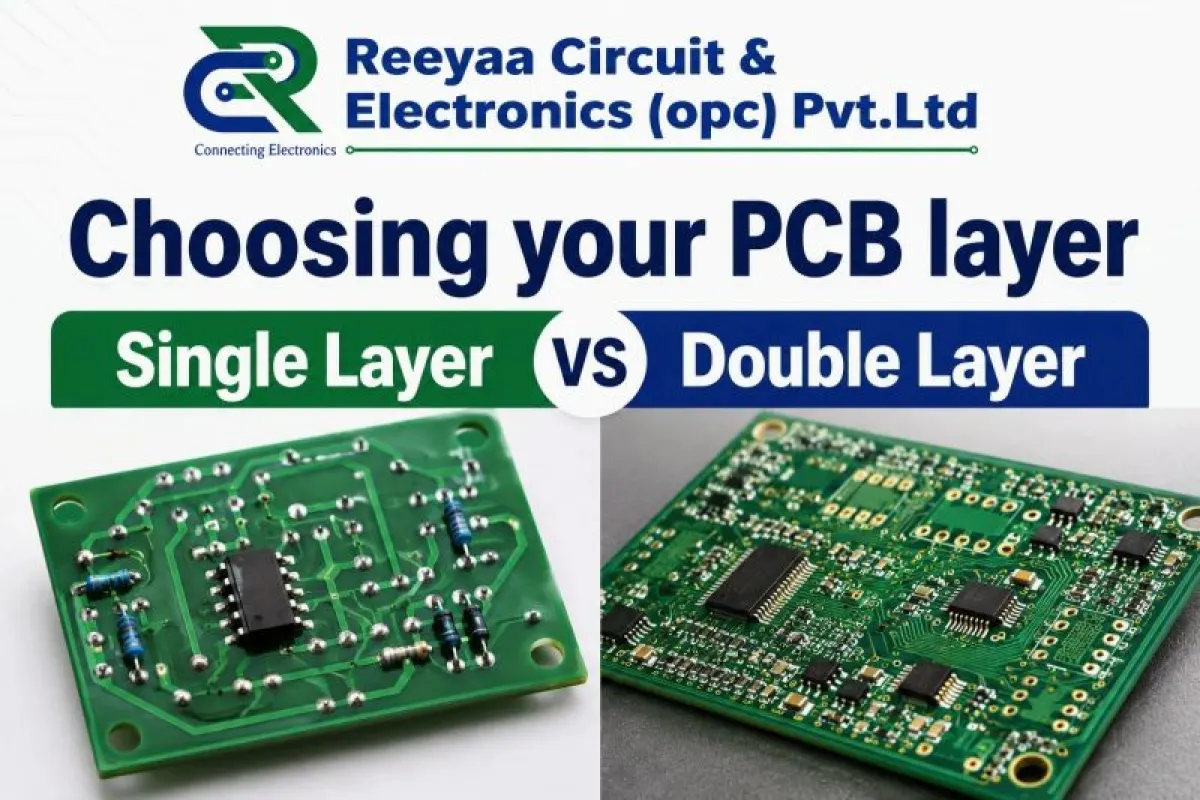
Single Layer vs Double Layer PCB: Which One Should You Choose?
Understand the differences between single-layer and double-layer PCBs, including cost, design complexity, space efficiency, and applications. Discover which PCB type best suits your electronic project.
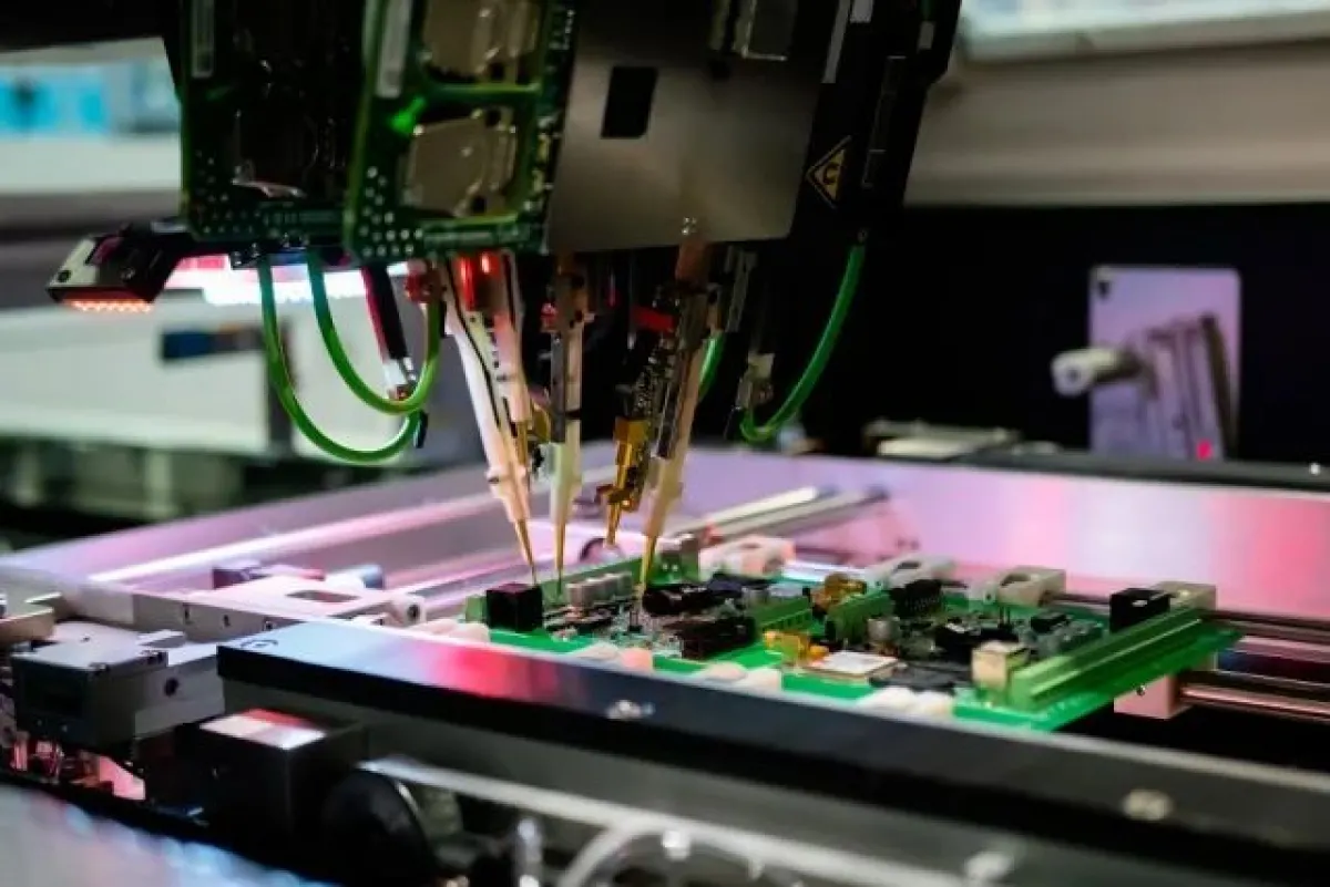
Flying Probe Testing (FPT): Ensuring PCB Quality at Reeyaa Circuit
Discover how Reeyaa Circuit uses Flying Probe Testing (FPT) to detect electrical opens and shorts in bare PCBs. Reliable electrical testing helps ensure PCB quality before component assembly.