
PCB Fabrication lead time
Every electronics product starts with one thing — a PCB.
But turning a design into a real board shouldn’t take weeks.
For hardware engineers, researchers, and startups, speed matters.
When you're testing a new circuit or debugging a prototype, waiting too long for PCB fabrication can delay the entire development cycle.
That’s why fast turnaround PCB fabrication is becoming critical for modern hardware development.
At reeyaacircuit.com, we support single and double-layer PCB fabrication with flexible turnaround options depending on project urgency:
• 1 Day
• 2 Day
• 3 Day
• 5 Day
• 7 Day
• 10 Day
• 15 Day
We support both prototype and bulk production, with capabilities like:
✔ Minimum trace width: 0.2 mm
✔ Minimum drill size: 0.3 mm
✔ Copper thickness: 35µm / 70µm
✔ Thickness options: 0.8 – 2.4 mm
All PCBs are electrically tested using FPT and BBT to ensure reliability.
Engineers can also order PCBs online directly through our ordering platform:👉 check out here: app.reeyaacircuit.com
Related Articles
Choosing the Right PCB Copper Weight: 1 oz vs 2 oz vs 3 oz
Learn the differences between 1 oz, 2 oz, and 3 oz PCB copper weights, including copper thickness, current-carrying capacity, trace width, and applications. Discover how to select the right copper weight for digital circuits, power supplies, motor controllers, and EV electronics.

PCB Manufacturing Process: From Gerber Files to Final Delivery
Discover how a PCB moves from Gerber file submission to final delivery. Learn about design rule checks, CAM engineering review, panelization, fabrication, electrical testing, and common causes of production delays.
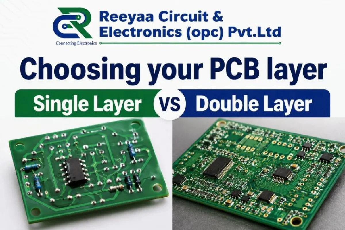
Single Layer vs Double Layer PCB: Which One Should You Choose?
Understand the differences between single-layer and double-layer PCBs, including cost, design complexity, space efficiency, and applications. Discover which PCB type best suits your electronic project.