
How PCB Fabrication Happens: A Step-by-Step Guide
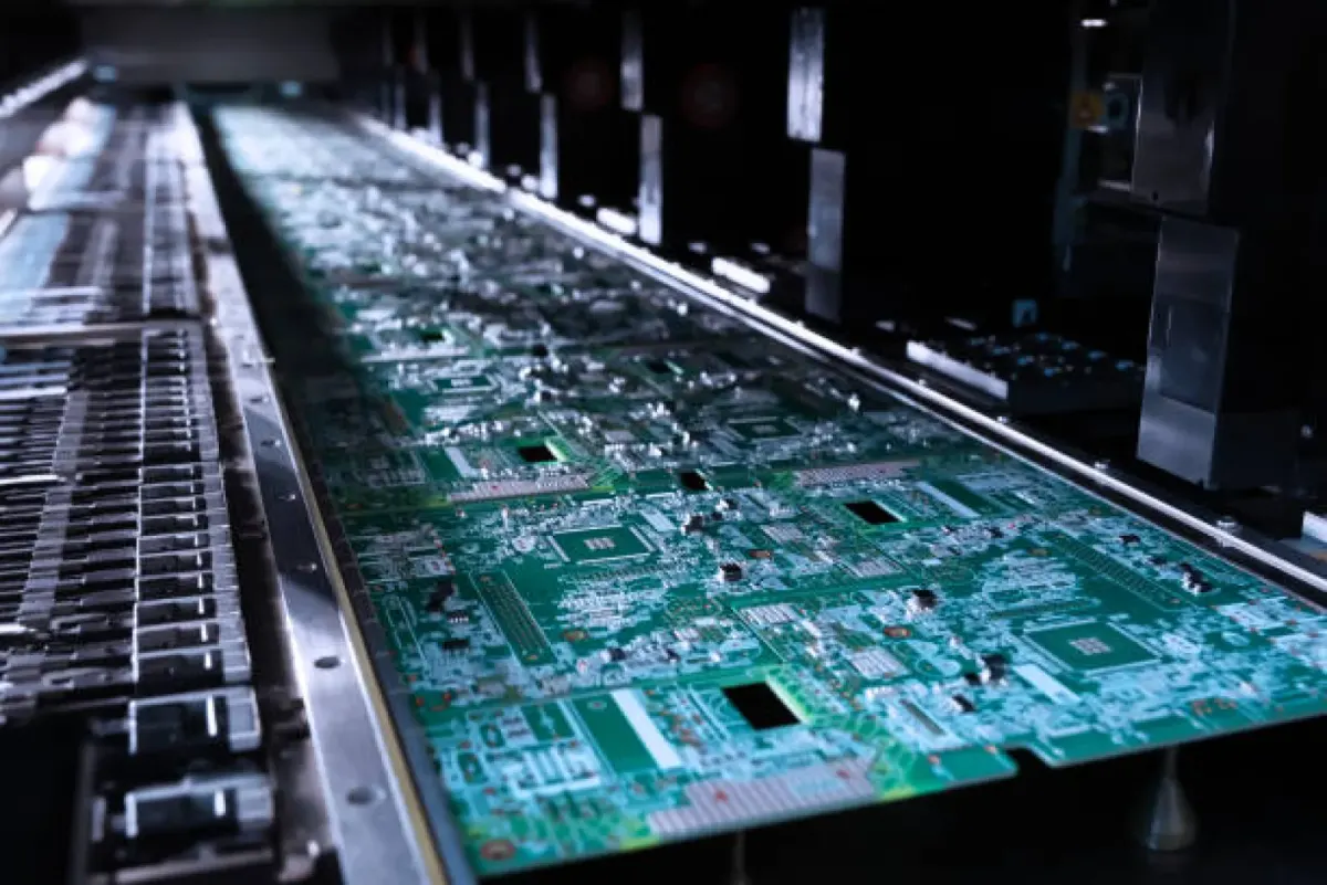
Printed Circuit Board (PCB) fabrication is the process of transforming a circuit design into a physical board that powers electronic devices. It begins with creating a PCB layout using CAD software, where engineers define component placement and electrical connections.
Next, the design is transferred onto a copper-clad laminate using a photoresist layer. The unwanted copper is removed through a chemical etching process, leaving only the required circuit traces. After etching, precision drilling creates holes for component leads and vias that connect different PCB layers.
The board then undergoes copper plating to improve electrical conductivity, followed by the application of a solder mask that protects the copper traces from oxidation and accidental short circuits. A silkscreen layer is added to display component labels, logos, and assembly markings.
Finally, every PCB is inspected and electrically tested to ensure it meets quality standards before assembly. Modern PCB fabrication combines advanced machinery with strict quality control, producing reliable circuit boards for consumer electronics, industrial equipment, automotive systems, and medical devices.
Understanding the PCB fabrication process helps engineers, students, and electronics enthusiasts appreciate the precision required to manufacture high-quality printed circuit boards.
Related Articles
What Information Should You Include with Your PCB Order?
Avoid PCB manufacturing delays and unnecessary costs by providing complete order details. Learn which Gerber files, board specifications, materials, copper thickness, surface finish, quantities, and special requirements to include when ordering PCBs.
PCB Panelization: How It Improves Manufacturing Efficiency
Discover how PCB panelization combines multiple circuit boards into a single manufacturing panel to improve production efficiency, simplify assembly, reduce handling, and optimize material usage. Learn about V-cuts, breakaway tabs, tooling holes, and fiducial marks.
Prototype PCB vs Production PCB: Key Differences Before Scaling
A working prototype doesn't always guarantee production success. Learn how design for manufacturability (DFM), component sourcing, manufacturing tolerances, electrical testing, and cost optimization help prepare your PCB for reliable mass production.